


Hastaş Beton
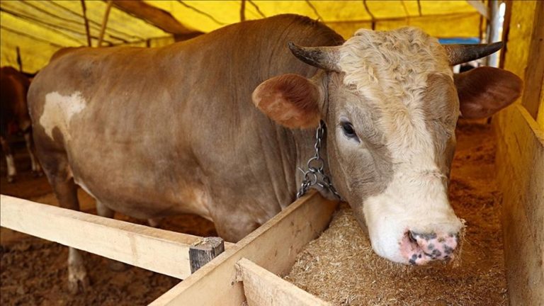
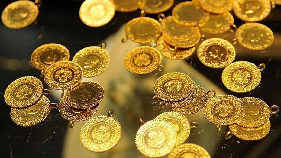
Kurbanlık fiyatları il il sorgulama ekranı 2026: Büyükbaş ve küçükbaş canlı kilo fiyatı ne kadar? İstanbul, Ankara, İzmir ve tüm illerin kurbanlık fiyatları
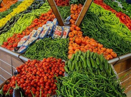
Antalya üretimde rakip tanımadı! 31 üründe Türkiye birincisi

Şans sektöründe doğru seçim Huqqabet
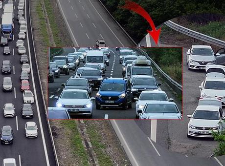
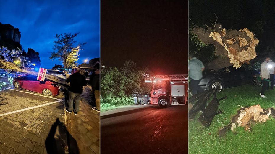
9 günlük bayram tatili için büyük göç başladı! İşte yollarda son durum
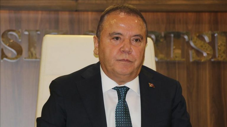
Mühittin Böcek’e ev hapsi kararı
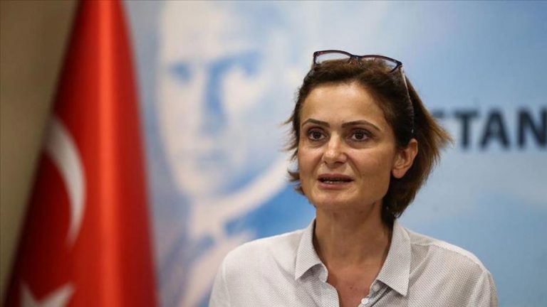
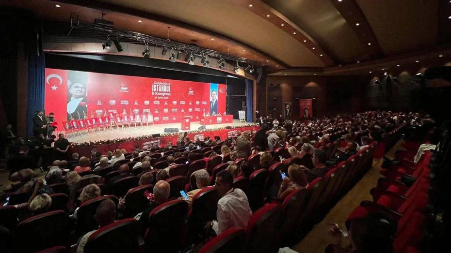
Canan Kaftancıoğlu için yakalama emri
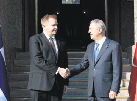
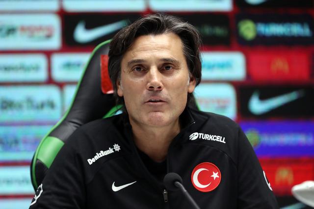
‘F-16 konusunda olumlu ve somut adım bekliyoruz’

Beşiktaş’ta Serdal Adalı’dan Şenol Güneş’e dair çarpıcı açıklama!

Ebru ve Zeynep’in hayatı tehlikede!

‘Dijitale erişememek ciddi bir yoksunluk’

2027 hac başvuruları için tarih belli oldu

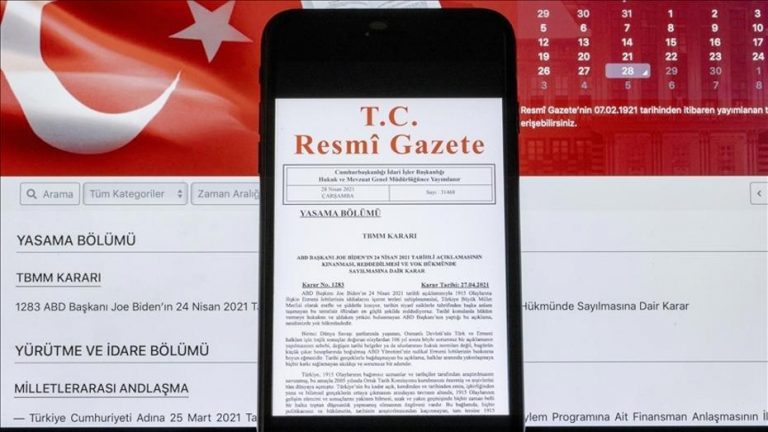
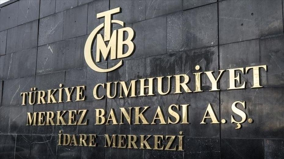
Merkez Bankası faiz kararı ne zaman? Ekonomistlerin nisan ayı faiz beklentisi belli oldu

Online Dünyada Siteni Oluştur Yolu
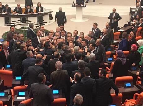
Bütçe maratonu gergin başladı! Vekiller birbirine girdi
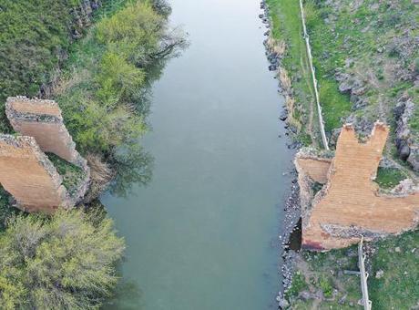
Türkiye Ermenistan ticaret kapısını açıyor
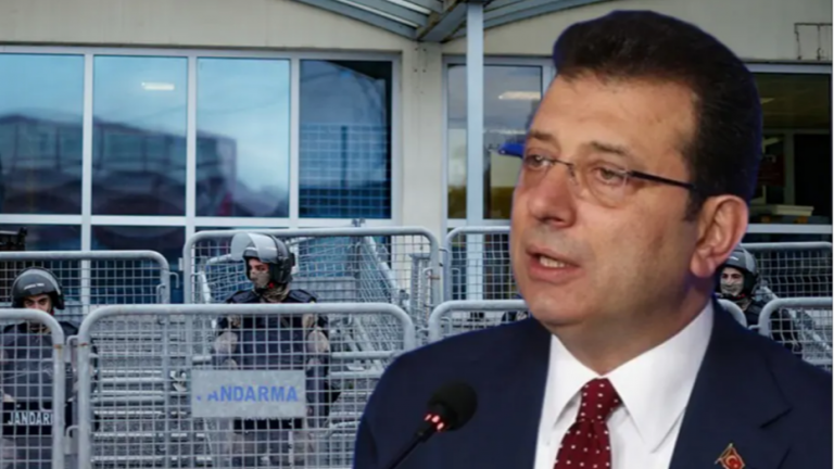
“Casusluk” davasında ara karar. İmamoğlu ve 3 sanığın tutukluluk halleri sürecek

Modern İletişim İçinde Yeni Nesil İletişim Sistemi talkrand
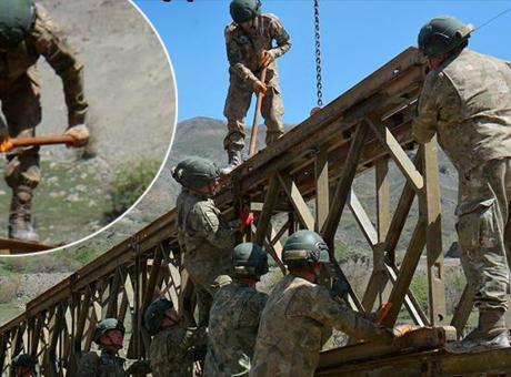
55 asker, 3 günde yaptı: Adı ‘Kaan’ oldu
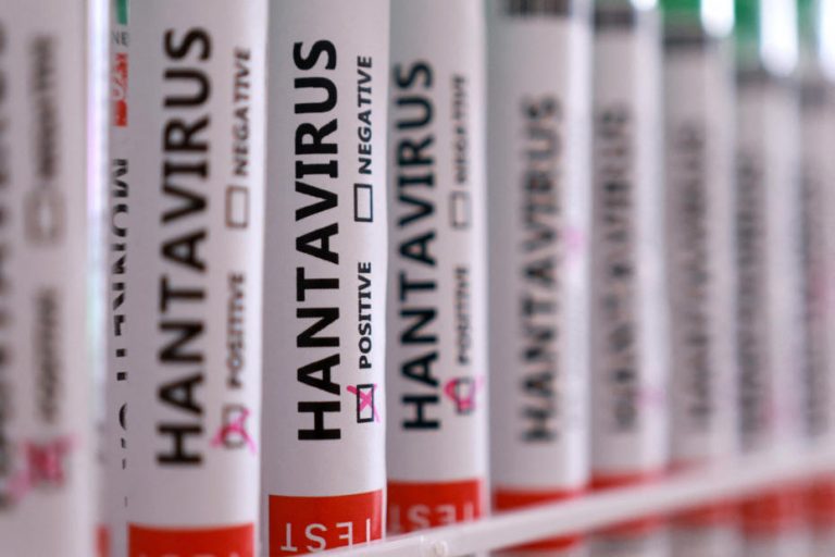
Türkiye’de hantavirüs vakası var mı? Sağlık Bakanlığı’ndan açıklama

Seda Sayan’dan can dostu Safiye Soyman itirafı: Dedikoducu!

Kaliteli Takı Dünyasında Farklı Bir Deneyim
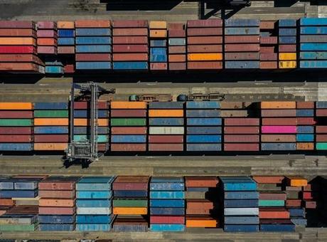
Makine ihracatına ‘Yapay Zeka’ dopingi